What’s the Best Coating for MEMS?
Posted by Sean Horn
Friday, December 11, 2015 7:59
@ 7:59 AM
Defining MEMS
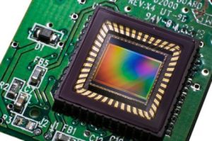
Microelectromechanical systems (MEMS) consist of technologies whose operative components range between 1-100 micrometers in size. The micronization of MEMS devices and structures (their mechanical and electro-mechanical elements) is a consequence of developments in modified semiconductor fabrication technologies originally used for electronics.
 The basic defining characteristic of MEMS is mechanical functionality, regardless of components ability to move physically within their product casing. However, this definition can be deceiving. Although some MEMS devices have no moving parts, many are complex electromechanical systems, with multiple moving elements managed by integrated microelectronics. Combining microelectronics, microactuators and microsensors with related technologies, thus integrating their functions onto a single microchip, is expected to be one of the future’s most significant technological breakthroughs.
Coating MEMS
MEMS products are frequently used in areas of high functional activity and stress. Prevailing environmental conditions can compel protection from exposure to temperature extremes, abrasive liquids, or similar circumstances that can generate product degradation or malfunction. Micronized components also frequently suffer from stiction — friction that interferes with stationary surfaces being set in motion during operation.
Under these conditions, it is necessary to protect components by depositing exceptionally thin films of covering material onto substrates during MEMS processing. Depending on the MEMS component and its uses, these coating layers may need to be as thin as five nanometers to effectively minimize stiction, while providing insulation and otherwise securing components’ functions. Coatings exceeding 100 micrometers interfere with components’ performance, rendering them ineffective for MEMS purposes.
Conventional liquid-phased, monolayer coating processes, such as spraying and dipping, have proven less useful for MEMS purposes. Vapor deposition processes are more effective for MEMS because they completely eliminate the wet deposition methods necessary for such coating materials as epoxy, silicone, or urethane. Thus, many conformal substances using these methods — acrylic, epoxy, silicon, urethane — have fewer applications for MEMS, unless they can be adapted to vapor-phased anti-stiction techniques, which are superior.
Mechanical deposition processes for MEMS include:
Physical Vapor Deposition (PVD): Of value for metal deposition, PVD coatings such as diamond-like carbon (DLC) generate low levels of stiction and high micro-hardness. However, film quality is inferior to chemical vapor deposition (CVD), with lower substrate adherence, higher resistivity, more defects and blemishes along surfaces. Limited and specialized application suggested.
Casting: Coating materials are dissolved in a solvent and applied to the substrate in liquid form by spraying or spinning. A thin film of coating material – organic photoresists, polymides, epoxy — remains on the substrate following solvent evaporation, in the range of tens of micrometers. Limited applications for polymers, metal and glass.
Chemical deposition processes for MEMS include:
Thermal Oxidation: This very very basic deposition technology is effective only for materials that can be oxidized. Temperature levels of 800°C -1100°C accelerate the coating process. Diffusion of oxygen into the surface can form silicon dioxide on a silicon substrate; substrate penetration improves electrical insulation. Unfortunately, coatings thicker than ~100 nanometers can generate additional surface films that restrict use for MEMS applications.
Electrodeposition: Limited to electrically-conductive materials, substrate surfaces may require a previously-applied electrically-conductive coating before deposition can be enacted. In these cases, electrodeposition generates reliable conformal coatings for metals such as copper, gold and nickel, at thicknesses of ~1µm to >100µm. However, film thickness and uniformity are difficult to control; limited application suggested.
{{cta(‘0ba42ac7-8bd7-476a-b346-2350a9cf8e85’)}}
Chemical vapor deposition (CVD): The most reliable MEMS coating technology, higher CVD process temperatures yield a coating surface of better quality, with fewer defects. Parylene stands out in this respect. Its conformal coatings are effective at thicknesses as slight as 0.1 microns, making them exceptionally adaptable for MEMS uses. Further beneficial qualities of CVD-deposited parylene include:
- uniform, pinhole-free surface-coverings for an exceptional diversity of substrate materials,
- dependable homogeneous barrier protection against acids, bodily fluids, chemicals, salts, solvents, water vapor, and other caustic solutions that are products of component operation,
- thermal stability between -200 °C to +350°C,
- electrical insulation,
- high tension strain,
- minimal dielectric constancy,
- ultraviolet protection, and
- suitability for an extreme diversity of complex coating conditions, ranging from exposed internal surfaces to substrates with crevices, points, or sharp edges.
Parylene’s CVD processes best assure precise MEMS-coating thicknesses, where even an additional micrometer of coating can generate component dysfunction or failure.
Conclusion
Semiconductor-made micro-mechanisms, MEMS demonstrate virtually unlimited potential for a multiplicity of rapidly evolving products: aerospace/automotive systems, consumer electronics, IT, telecommunications, and medically biocompatible/implantable materials’ uses, as well as ruggedized military applications of all types. Capacities for further product development and sophistication of MEMS are expected to proliferate in the future.
Because of their size and need to function through a diversity of frequently difficult conditions, MEMS components require exceptional protection. CVD-applied coatings provide the most durable and flexible coatings, able to withstand an extreme range of problematic operating conditions. Of available coating materials, parylene is the most widely used and the most reliable.
If you’re looking for conformal coating services for MEMs, contact Diamond-MT today. Get started by calling us at 814-535-3505 or completing a quote request.
Comments
Homepage 4/17/2020. 10:17:10 AM
... [Trackback] [...] Informations on that Topic: blog.paryleneconformalcoating.com/whats-the-difference-between-potting-and-conformal-coating/ [...]
londondrugscanada.bigcartel.comlondon-drugs 4/17/2020. 10:17:10 AM
cialis uk https://londondrugscanada.bigcartel.com/london-drugs This is nicely expressed. !