Can I Solder Through Parylene?
Posted by Sean Horn
Friday, July 20, 2018 7:30
@ 7:30 AM
Parylene: Properties and Processes
Conformal coatings are applied to printed circuit boards (PCBs) and other sensitive electronics to protect their components and electrical function. Parylene (XY) polymer provides these assemblies superb security from electrostatic discharge, and additional performance advantages, including:
- biostability,
- dependable corrosion/moisture resistance,
- good dielectric strength/high-frequency properties, with diminished dielectric constant,
- high bulk/surface resistance, and
- lowered kinetic/static coefficients of friction, while
- withstanding incursion of chemicals/solvents, salt spray, temperature fluctuations, and vibration,
- for a truly conformal pinhole-free coating that configures to any assembly topography.
These characteristics are adaptable to a wide range of as aerospace/defense, automotive, consumer, industrial, medical and public-service applications.
XY’s distinctive chemical vapor deposition (CVD) method of film application is the source of these performance advantages. Unlike the brush, dip or spray processes used to apply pre-synthesized liquid coatings – acrylic, epoxy, silicone, urethane – to substrates, CVD transforms solid parylene into a gas, which synthesizes during transformation onto targeted surfaces as a conformal coating. Implemented within a specially designed vacuum chamber held at room temperature, XY’s gaseous state seeps into a substrate’s surface, settling upon it as well, essentially growing the protective layer molecule by molecule. Length of exposure to the vaporized XY determines coating thickness, which grows incrementally with prolonged contact. The resultant conformal coating adheres to any PCB/assembly configuration, both internally and externally, generating exceptional protection.
Soldering Parylene
Once applied, XY is very difficult to remove, enhancing its protective/barrier utility. With regard to solder already in place on PCBS, XY film protection will expand its operational lifetime by as much as 100%, doubling the functional use of an assembly’s soldered joints and components.
Parylene also significantly limits the development of tin whiskers — microscopic conductive fibers growing from an assembly’s tin surfaces:
- a serious problem to its electronic performance,
- shorting out conductors during use,
- rendering the assembly is useless.
Solders composed at least partially from lead – the source of tin – are frequently used on PCBs, which can also have tin-plated surfaces. In comparison to liquid coatings, XY offers considerably better tin whisker protection, limiting its development while maintaining electrical functional, with much thinner layers of film.
But these are instances of parylene working in conjunction with already-soldered parts. Like other conformal coatings, application of XY is completed after boards have been manufactured; it cannot provide optimal performance for assemblies that require further soldering or other modification after film application. Yes,
- parylene can be successfully soldered through at any point after the conformal film has been applied,
- but doing so forces other issues,
- emanating from exposure of the already-covered substrate.
Because XY is so difficult to remove, soldering the coating surface should be confined to its removal, cases where PCB components are malfunctioning, or other repair issues emerge. XY’s CVD application method combines with its relative film durability to negate use of most removal methods available to liquid coating materials. For instance, XY cannot be simply be submerged in a solvent bath for removal, as is the case for a substrates coated with acrylic. Parylene removal is more difficult, requiring application of micro-abrasive, mechanical or focused heat (thermal) technologies.
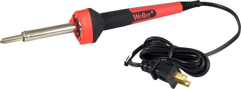
Despite difficulty removing parylene, concentrating extreme heat onto its conformal films will melt or burn through the film layer to the substrate. Thermal breach of the coating will occur regardless of its thickness. How long the process takes is a function of coating thickness; thicker coats will take longer to burn through. And remember, parylene has a higher melting point than many plastics, ranging from 290C for parylene C to nearly 500C for parylene D, N, and F. Under these circumstances, thermal application may take some time. Soldering will generate sufficient heat for these purposes; the handheld iron can be explicitly directed toward a designated region of the film’s surface.
This method of XY removal is, however, less advantageous than abrasive or mechanical methods. Soldering through parylene can:
- cause discoloration,
- yield residues,
- raise toxic fumes dangerous to the operator and, most significantly,
- damage PCBs and temperature-sensitive substrates,
- causing dysfunction or assembly failure.
Parylene can be soldered through. It is suggested that a highest-quality soldering iron under a vacuum hood be used for these purposes. Be aware of the consequences to the coating and perhaps the assembly itself if appropriate care is not taken. Commencing soldering processes should be confined to coating removal or assembly repair, since the heat generated by soldering can damage the substrate and its contents.
To learn more about parylene and how it can be processed, download our whitepaper now:
Download our guide on Parylene 101
Comments
Homepage 4/17/2020. 10:17:10 AM
... [Trackback] [...] Informations on that Topic: blog.paryleneconformalcoating.com/whats-the-difference-between-potting-and-conformal-coating/ [...]
londondrugscanada.bigcartel.comlondon-drugs 4/17/2020. 10:17:10 AM
cialis uk https://londondrugscanada.bigcartel.com/london-drugs This is nicely expressed. !