Nonconformity of Parylene on Wafers
Posted by Sean Horn
Friday, June 22, 2018 7:30
@ 7:30 AM
The polymer parylene (XY) provides exemplary, ultra-thin conformal coating for printed circuit boards (PCBs), solar cells, light emitting diodes (LEDs), medical implants, aeronautical/military equipment and numerous other products, with uniform, insulative protection in the nanometer (nm.) range.
One of XY’s basic advantages is its reliable coating uniformity, exceeding that of liquid materials like acrylic, epoxy, silicone and urethane. Rather than brushing dipping or spraying pre-synthesized layers onto substrates, parylene’s chemical vapor deposition (CVD) application method synthesizes the conformal film in process. Parylene’s deposition system consists of a series of vacuum chambers that sequentially produce parylene vapor, pyrolyze it, deposit it as a polymer, and then capture its effluent.
 Parylene is unique in being created directly on the surface at room temperature, and is widely regarded as the ultimate conformal coating for protection of devices, components and surfaces in electronics, instrumentation, aerospace, medical and engineering industries. In process, gaseous XY seeps deep into the substrate surface as well as building coating protection along its exterior, generating a double layer of conformal protection. Coating layers are far thinner than those provided by liquid materials, enhancing parylene’s functional versatility.
Nevertheless, XY’s layer uniformity is not always precise. This is far more often the result of deviation or non-conformity along the substrate surface than because of defects with the parylene material or the CVD process. This is not to suggest that:
- XY materials are always perfect,
- either in the raw dimer state
- or after transition to the vaporous entity that solidifies into parylene conformal film,
- or that CVD always proceeds faultlessly, without error.
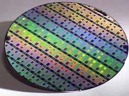
Problems do occur with both material and process, especially if the wrong XY type – C, N, F D, etc. — is selected for a coating assignment when another parylene variety will provide better coverage. However, deviations in parylene uniformity are far more frequently generated by variations in substrate topography. In these cases, parylene consistently provides an effective conformal coat. But there are instances where substrate features interfere with the overall and precise uniformity of the deposited XY film. Surfaces of semiconductor wafers can cause this problem to develop.
Moreover, the surface geography of semiconductor and sensor wafers is not a defect, but typical of their structure. According to international software engineering standard ISO/IEC 25010, it does not qualify as defective nonconformity or nonfulfillment of a quality requirement for intended usage. Indeed, standard wafer topography tends to be varied and is essential to its quality performance, particularly for wafers containing multiple chips. The parylene deposition process is the most efficient for accommodating these surfaces, since its vaporous consistency surrounds all areas on the wafer’s surface, penetrating within as well as forming a protective outer film layer.
Evidence repeatedly demonstrates CVD’s extreme utility as a method of thin film deposition on wafer and other similarly irregular substrates. XY’s prominence as a conformal coating rests largely on its ability to effectively cover component configurations with sharp edges, points, flat surfaces, crevices or exposed internal surfaces; normally, these are coated uniformly without voids. There are exceptions. While coating wafers will be complete in terms of coverage, a tendency toward minimal non-uniformity can develop.
Because of the exceptionally thin coating layers provided by parylene, non-uniformity will similarly be slight. A recent study showed that, through nine samples, average deviation in coating uniformity did not exceed –1.0 nm. or +1.5 nm., across the entire production run. Coating thicknesses also varied slightly according to which shelf in the deposition chamber the wafer was situated during CVD. The highest of the three deposition shelves averaged a coating thickness of 274.35 nm., the thinnest layer of the batch, perhaps because there were no obstacles above the sample situated at this level obstructing its vaporous movement. Layers were progressively thicker on the lower shelves; the middle shelf averaged 295.12 nm., the bottom and most spatially-confined shelf, 308.52 nm.; there was less room for the vaporous XY to circulate there, causing it to settle on the wafer’s surface.
Thin conformal films generated by parylene CVD tend typically to be exceptionally uniform, even in the nm. range. However, research evidence shows that differences in both
- coating deposition rate and
- resultant film thicknesses are not uncommon,
- even within a single product batch.
For wafers, a deposition footprint can emerge, wherein coating uniformity in the wafer’s center deviated to the extent that film thicknesses were slightly greater at substrate boundaries and wafer edges/rims. Development of shadowing —
- uneven film coverage in those PCB regions where component topographies are closely situated or overlap, or
- elements of application structures – for instance, sample shelves – physically obstruct parylene access –
can occur if the CVD process is not appropriately monitored. CVD processing of semiconductor wafers offer a rare instance where non-uniform parylene deposition occurs, although at an insufficient level to effect unit protection or function.
To discover more about parylene and MEMS, download our whitepaper now!
Download our guide on Parylene 101
Comments
Homepage 4/17/2020. 10:17:10 AM
... [Trackback] [...] Informations on that Topic: blog.paryleneconformalcoating.com/whats-the-difference-between-potting-and-conformal-coating/ [...]
londondrugscanada.bigcartel.comlondon-drugs 4/17/2020. 10:17:10 AM
cialis uk https://londondrugscanada.bigcartel.com/london-drugs This is nicely expressed. !