Does Parylene Get Everywhere?
Posted by Sean Horn
Friday, April 27, 2018 7:30
@ 7:30 AM
After pertinent research you’ve determined parylene (XY) is the best conformal film for your coating assignment. Especially relevant were XY’s uniform protective and insulative properties, which are useful for numerous applications, ranging from printed-circuit boards (PCBs) to medical implants to military-grade purposes. Among parylene’s other advantages are:
- adherence to an exceptional quantity of substrate geometries/materials,
- biological/chemical inertness,
- bubble- and pinhole-free conformability/flexibility at film thicknesses greater than 0.5 microns,
- excellent dielectric/moisture barrier properties,
- high optical clarity,
- penetration of extremely small crevices/spaces,
- tin whisker mitigation, and
- withstanding autoclave-level heat
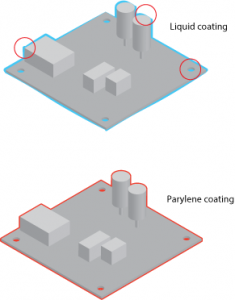
Applied through a chemical vapor deposition (CVD) process, gaseous XY s can be deployed and adhere on any surface that touches air. Thus, it has the capacity to coat under components, inside minute substrate fissures, and inside semi-sealed areas. Unlike liquid film materials, the micron-level thinness of parylene films generate coatings without forming bridges in tight areas.
These properties have been verified repeatedly through parylene’s use and have been extended as application technologies improve. But, for your own coating assignments, you need to know if the parylene film reaches and adheres everywhere required by the coating assignment’s specifications. You’ll want the most reliable proof available of the coating’s absolute conformality.
Verifying Parylene Conformality
 Verifying XY conformality – the property of uniform parylene application throughout the project-specified surface for each coated assembly — may require specialized inspection methods. With greater resolution power than a light microscope, electron microscopy (EM) offers much higher magnification than most alternatives; it permits finely-detailed views of much smaller objects, like XY’s many microelectricalmechanical systems (MEMS)/nano-tech applications. EM uses a beam of electrons –stable, negatively-charged subatomic particles found in all atoms, the primary carrier of electricity in solids — to create an image of the specimen. This technique can provide images suitable for confirming XY conformality.
However, additional methods may be required. Physically-cleaving a coated specimen where XY film thickness exceeds 200 nanometers (nm) allows more precise imaging; cross-sectional scanning electron microscopy (SEM) will generate images suitable for conformality determination. SEM images show how well the parylene has coated the specimen, and
- if the coating thickness is pinhole-free/uniform, or
- where any gaps in the coating exist.
Sequential cross-sectioning helps determine conformality (or its lack) along the surface of a single specimen or through an entire sample.
Physical cross sectioning may not work for all substrate topographies. Use of ion/electron beam ablation (I/EBA) can successfully image the XY film/substrate interface, to determine if the parylene has indeed adhered everywhere intended by the coating assignment’s specifications.
Verifying XY conformality becomes proportionally more difficult as coating layers decrease in size, as with MEMS/nano-tech applications, where layers frequently are less than 100 nm. Analysis of SEM cross-sectioning becomes more difficult under these circumstances, suffering from Z-contrast/charging effect inconsistency. These conditions can be rectified using a focus ion beam (FIB) system in conjunction with transmission electron microscopy (TEM). TEM is used to view thin specimens – like tissue sections, molecules, in addition to conformal layers — through which electrons can pass generating a projection image.
Electron microprobe analysis (EMPA) can enrich TEM imagery. Working similarly to an SEM, EMPA is an analytical tool used to non-destructively determine the chemical composition of small volumes of solid materials. While this technique is adept at verifying the conformality of thinner, more complex layers of parylene, its accuracy can be challenged by ion damage, as film thicknesses diminish (>20 nm).
In such cases, using SEM images prior to- and following CVD can generate a reasonable view of coating covering and conformality. This technique is valuable in cases characterized by property changes to the substrate surface initiated by CVD. Such applications – where preservation of the precursor functionality down the depth of feature is necessary – benefit from combined (before/after) SEM imaging. Comparing prior-with-final assembly properties verify applied XY conformality in these cases.
A Simple Solution
These methods will be very useful in determining the exact placement of Parylene at different levels of the object that was coated. For most applications, simply looking at the areas that have been de-masked, as we discussed in the how to inspect Parylene article. If you can see the de-mask lines, take solace in the fact that coating HAS to be on the rest of the board. It simply cannot NOT be there.
To learn more about Parylene inspection, download our whitepaper now:
{{cta(‘d5742a7f-cdfa-484e-9920-e8698c8e12e0’)}}
Comments
Homepage 4/17/2020. 10:17:10 AM
... [Trackback] [...] Informations on that Topic: blog.paryleneconformalcoating.com/whats-the-difference-between-potting-and-conformal-coating/ [...]
londondrugscanada.bigcartel.comlondon-drugs 4/17/2020. 10:17:10 AM
cialis uk https://londondrugscanada.bigcartel.com/london-drugs This is nicely expressed. !