Can Parylene Be Layered?
Posted by Sean Horn
Friday, October 2, 2020 8:00
@ 8:00 AM
Multilayer conformal coatings are advantageous in resolving diffusion or stability issues. A vast amount of knowledge is available in the literature about the use of multilayered stacks of parylene and stacks making use of different intermediate materials such as metals and so on. Use of multiple layers of parylene C was most commonly reported for medical implants [1].
Adhesion
Surface energies of materials affect the molecular force of attraction. High surface energy (HSE) leads to a strong molecular attraction and they are easier to bond, whereas a low surface energy (LSE) means a weak molecular attraction [2]. Most polymers possess low surface free energy and they lack polar functional groups on their surface that results in poor adhesion properties [3]. LSE of Parylene also makes it an excellent protection layer against oxidants, corrosives. Parylene C has a contact angle of ≈90 degrees [4].
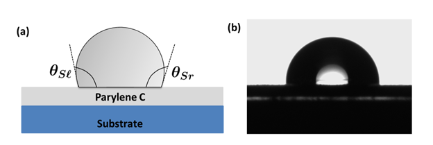
Figure 1 (a) Schematic of a water droplet on a Parylene C surface (b) Photograph of a water droplet on the Parylene C film [4].
Parylene/Parylene interface
As explained above, the common issue for parylene on top of parylene is the adhesion problem. While in situ parylene coating one after each other without exposure to outside world may improve the result, usually the parylene layer is exposed to outside world for other processes which results in the deposition of organics on the surface of the bottom parylene layer (changing the polarity of the surface) resulting in additional adhesion issues. Parylene/parylene interface must be clean and activated to be successfully formed. Therefore, requires further cleaning and surface treatment such as oxygen plasma. In one of the studies annealing at 200°C (above the glass transition temperature of parylene-C) was shown to improve the adhesion force between two parylene C layers. At 200°C recrystallization and intermolecular mixing increases. It is important to remind that the glass transition temperature of parylene is 90 °C. Minimizing the use of high temperature (>100 °C) processes can prevent oxidization, thermal stress, the formation of gas bubbles, or irreversible changes to parylene morphology [5]. A number of tests have been done on the adhesion of parylene to parylene using different surface treatments as shown in the schematic. The process starts off with a silicon wafer which is cleaned by a BHF solution followed by the first parylene layer deposition. Among the six methods Propylene Carbonate was found to be most useful by the researchers.
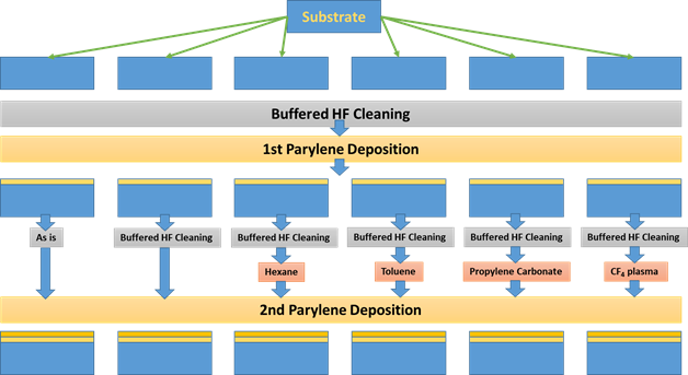
Figure 2 Treatment for interface of Parylene/Parylene adhesion [6].
Parylene/Intermediate Layer/Parylene interfaces: Polymer, Metal, Oxide, Nitride etc.
The adhesion of parylene on top of other materials require pre-processing of the parylene layer. Different methods have been proposed in the literature: Silicon XeF2 surface roughening (with 6.5 μm of silicon removal), parylene anchoring using advanced DRIE techniques, parylene melting at 350°C, and A-174 adhesion promoter were suggested [6] Most of these techniques are not applicable to parylene to parylene, or parylene to metal but parylene to silicon.
Also, parylene suffers from poor adhesion to noble metals, gold and platinum, which makes it an important bottleneck in the implementation of parylene in different applications (medical implants, electrodes, sensors, etc.). Once the manufactured device of a multilayered structure is soaked in wet environments weak adhesion between different layers might lead to catastrophic failure of parylene devices due to electrical shorts and delamination.
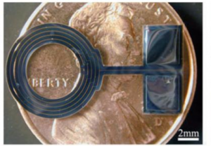
Figure 3 Dual metal layer coil sitting on a penny [7].
Atomic layer deposition (ALD) of Al2O3 was scientifically shown to be feasible and was reported to form a good bond at the interface between ALD- Al2O3 and the Parylene C layer [8].
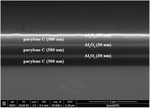
Figure 4 SEM image of cross-section of organic/inorganic multilayer structure. Bright films are 30 nm-thick Al2O3 and dark films are 500 nm-thick parylene [9].
In conclusion, multilayers of parylene/parylene or parylene/material systems can be produced but careful consideration while choosing the materials must be given to the surface treatment conditions, to adhesion promoters and to the surface energy must be given. Otherwise, delamination and resultant catastrophic failure is inevitable.
Discover more about parylene coating by downloading our whitepaper.
References
[1] D. Ziegler, T. Suzuki, and S. Takeuchi, “Fabrication of Flexible Neural Probes With Built-In Microfluidic Channels by Thermal Bonding of Parylene,” J. Microelectromechanical Syst., vol. 15, no. 6, pp. 1477–1482, Dec. 2006, doi: 10.1109/JMEMS.2006.879681.
[2] “What Does Surface Energy Mean and Why Is It Important?,” BDK, Aug. 01, 2018. https://www.bdk.uk.com/2018/08/surface-energy-why-important-adhesive-selection/ (accessed Jun. 25, 2020).
[3] F. Awaja, M. Gilbert, G. Kelly, B. Fox, and P. J. Pigram, “Adhesion of polymers,” Prog. Polym. Sci., vol. 34, no. 9, pp. 948–968, Sep. 2009, doi: 10.1016/j.progpolymsci.2009.04.007.
[4] C. Chindam, A. Lakhtakia, and O. O. Awadelkarim, “Surface energy of Parylene C,” Mater. Lett., vol. 153, pp. 18–19, Aug. 2015, doi: 10.1016/j.matlet.2015.04.009.
[5] J. Ortigoza-Diaz et al., “Techniques and Considerations in the Microfabrication of Parylene C Microelectromechanical Systems,” Micromachines, vol. 9, no. 9, Art. no. 9, Sep. 2018, doi: 10.3390/mi9090422.
[6] J. H.-C. Chang, B. Lu, and Y.-C. Tai, “Adhesion-enhancing surface treatments for parylene deposition,” in 2011 16th International Solid-State Sensors, Actuators and Microsystems Conference, Jun. 2011, pp. 390–393, doi: 10.1109/TRANSDUCERS.2011.5969484.
[7] N. Islam, Microelectromechanical Systems and Devices. BoD – Books on Demand, 2012.
[8] J. Njeim et al., “Effect of the Al2O3 Deposition Method on Parylene C: Highlights on a Nanopillar-Shaped Surface,” ACS Omega, Jun. 2020, doi: 10.1021/acsomega.0c00735.
[9] J. Wu et al., “Efficient multi-barrier thin film encapsulation of OLED using alternating Al 2 O 3 and polymer layers,” RSC Adv., vol. 8, no. 11, pp. 5721–5727, 2018, doi: 10.1039/C8RA00023A.
Comments
Homepage 4/17/2020. 10:17:10 AM
... [Trackback] [...] Informations on that Topic: blog.paryleneconformalcoating.com/whats-the-difference-between-potting-and-conformal-coating/ [...]
londondrugscanada.bigcartel.comlondon-drugs 4/17/2020. 10:17:10 AM
cialis uk https://londondrugscanada.bigcartel.com/london-drugs This is nicely expressed. !