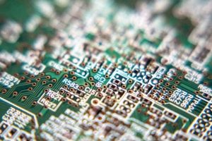
Repairing Parylene Coated PCBs
Posted by Sean Horn
Friday, September 30, 2016 7:30
@ 7:30 AM
Parylene’s CVD method of application generates exceptionally lightweight yet durable conformal coatings, with superior barrier properties. Compared to liquid processes, the effects of gravity and surface tension are negligible, so there is no bridging, thin-out, pinholes, puddling, run-off or sagging.
Typically, parylene films measure between 500 angstroms to 500 microns in thickness; these ultrathin films eliminate performance complications arising from excessive coating mass or viscosity, conditions that might interfere with components’ function. The resultant protective layers maintain the performance capabilities that distinguish parylene from liquid competitors; for instance, a 25 micron coating will have a dielectric capability in excess of 7,000 volts.
Because parylene provides unparalleled component protection at film thicknesses far thinner than competing wet coatings, it is the coating of choice for many MEMs/nano technologies. Offering unsurpassed protection for numerous current conformal coating applications – aerospace, LED, medical, military, and a range of ruggedized products — parylene films ensure high reliability and longer life for customer-end products; they diminish total costs for maintenance, repair and replacement, for producers and end-users. However, this does not mean the coatings themselves are flawless; they occasionally require repair.
Enacting Parylene Coating Repair
The unique CVD process that provides parylene with many of its advantages as a conformal coating also serves as a barrier to reworking the coatings. Circuit repair of parylene coatings is characterized by unique issues, emanating from parylene’s divergence from more conventional wet coating types. Reliably strong and hard, parylene coatings are exceptionally difficult to chip away or otherwise mechanically compromise; all covered surfaces are typically resistant when reworking is necessary.

Whereas acrylic- or silicone-based coatings use selective spot- or overall dip-exposure solvent-application methods for ready removal from PCBs, parylene’s specialized CVD coating technique results in film thickness and surface qualities that do not respond to these treatments. Similarly, parylene rework/removal cannot be accomplished as reliably through the thermal/physical deletion techniques typically applied for epoxy or urethane.
Resisting organic solvents, parylene’s removal is further complicated by melting or burning temperatures in excess of 350°C (higher in a vacuum), which generally exceed those of the plastic substances composing at least part of the PCB’s structure. Just as specialized vacuum chamber equipment is required to apply parylene conformal films to assembly substrates, equally specialized methods – such as plasma etching or micro-blast abrasion – are necessary to safely remove parylene from the same surfaces. In addition,
- repair of parylene coated PCBs generally requires recoating with parylene, rather than wet technique conformal films, although
- if an appropriate primer is used, lower-priced, field-friendly substances like flexible polyurethanes can assist the repair process.
Where rework is necessary, incision and removal techniques can also treat the parylene surface. This is a mechanical process involving cutting into the treatment surface to initiate separation of the film from the substrate, followed by lifting the damaged parylene with tweezers or a similar device. Although incision removal is often manual, it is suggested operators wear protective gloves. Human flesh contacting the surface to-be-reworked will invariably leave a residue of bodily fluid (oil, perspiration, etc.), which will require additional specialized removal, further complicating the rework process.
It should be noted that, in many cases, repair does NOT entail stripping the board entirely. It is more likely that spot removal of the parylene coating will be required for localized repair of a minute assembly component; typically, the item needing repair is so small that stripping the entire board is unnecessary, costlier and time-consuming. Under these circumstances removal is readily accomplished by using a soldering iron to burn through the parylene surface, affecting the repair, and touching-up the area with a liquid conformal coating; urethane is used most frequently under these circumstances. Of course, care must be taken: Localized application of extreme heat, such as with a soldering iron, can, in fact, melt or burn through a parylene conformal coating.
Whatever technique is employed, the objective is to strip the damaged parylene from the substrate and efficiently replace it to a state where assembly function can be maintained. Reworked/removed parylene cam frequently be recoated to original specifications.
Summary
Durable and heat/solvent-resistant, parylene is difficult to remove or rework. CVD generated substrate penetration significantly increases problems simply peeling the parylene film from the surface. Parylene can be removed for PCB rework by one of several methods. Among the most common removal techniques are, incision/deletion, laser ablation, mechanical or micro-blast abrasion, plasma etching, and thermal softening.
The optimum process of removal is determined by the nature of the device and the particular needs of the client or end-user. Perhaps the best approach is avoiding the need to rework, by appropriately:
- cleaning the substrate,
- masking the assembly properly prior to deposition,
- ensuring a reliable connection between parylene type and substrate material,
Furthermore, after parylene removal, it is essential to develop machining parameters that will not cause damage to the specific PCBs being reworked. In this respect, thoroughly reviewing data sheets and related information for all assembly components requiring rework is recommended; equally important is establishing consistent performance standards for electrostatic discharge (ESD, a source of electrical shorts or dielectric breakdown), process management, and working temperatures. Rework that proceeds without adhering to these basic guidelines can become the source for future rework. Every case is different, so the rework process will require controlled customization. However, in many cases, areas where parylene has been removed can be recoated to conform to original design parameters.
To learn more about common parylene problems and how to prevent them, download our whitepaper now:
{{cta(‘67972768-ab7a-4367-83ee-db9ddf93913c’)}}
Comments
Homepage 4/17/2020. 10:17:10 AM
... [Trackback] [...] Informations on that Topic: blog.paryleneconformalcoating.com/whats-the-difference-between-potting-and-conformal-coating/ [...]

londondrugscanada.bigcartel.comlondon-drugs 4/17/2020. 10:17:10 AM
cialis uk https://londondrugscanada.bigcartel.com/london-drugs This is nicely expressed. !