Why does the parylene process take so long?
Posted by Sean Horn
Friday, March 6, 2020 1:38
@ 1:38 PM
Parylene is a transparent polymer that offers uniform and pinhole-free conformal coatings for printed circuit boards, medical devices, and microelectronics. Varieties of parylene are made available through a modification of the molecular structure of para-xylylene (Parylene N, C, D, and F-AF4, and F-VT4). Each modification results in a set of material properties that are applicable in different service conditions.
There are a number of point of consideration which shall be kept in mind for parylene process from start to end. Parylene coating process is an engineering intensive advanced process which results in a very high quality advanced conformal coating. Each step of the handling and processing is done with care and precision (Fig. 1).
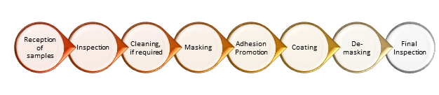
Figure 1 Process flow of parylene coating from start to end.
Reception of samples: Parylene related processes starts with the reception of the sample substrates to be coated. The number of samples and surface area are deterministic in the deposition process time.
Inspection: After the reception, samples are inspected for their surface quality, cleanliness and any damages.
Cleaning and surface activation: Sometimes, samples require a surface cleaning process such as basic plasma cleaning processes (oxygen plasma) or UV-ozone treatment for surface activation. This process might take from a few minutes to an hour depending on the severity of organic contamination and residues adhering to the substrate surfaces. In some cases, wet cleaning might be required prior to the plasma activation. The quality of the bond surface is of very high importance in parylene conformal coatings final quality. The adhesion strength is highly dependent on the surface energy of the substrate and organic residues results in a low surface energy which is not favorable in interface formation. In summary, dirty surfaces prevent parylene molecules from attaching and penetrating to the substrate’s crevices and pores.
Masking: Masking is a critical step, especially in microelectronics, because this step determines the available surface areas for parylene deposition. For example, for MEMS processes the backside of the silicon or SOI wafers might be required to be left free of parylene. PCB’s can be protected against parylene deposition using a masking tape. Mask is applied according to a pre-determined and drawn masking drawing.
Masking must be done by a professional making sure of a uniform application without any holes and paths where the parylene can penetrate. Because parylene molecules can enter and diffuse into very small holes and pores of a few hundred nanometers masked areas should be carefully examined prior to taking the samples to the CVD processing chamber. It must be clear that masking can take a significant time depending on the number of samples.
Silane A-174 and surface adhesion promoters: To improve the adhesion on the target surface extra care is taken to clean the surface. Subsequently, the samples surfaces are treated using an adhesion promoter such as a silane (A-174). Adhesion promoter forms a monolayer of molecules in a way to provide a high strength bond interface between the surface and the parylene. This step can be done in the vapor phase in the processing chamber.
Deposition (CVD):
The chemical vapor deposition (CVD) process of parylene takes place in three steps (sublimation, pyrolysis, deposition). Overall the process might take from a few hours to over 24 hours depending on the coating thickness and equipment related processes such as chill time for the cold trap (approximately 30 minutes), reaching the right temperature and pressure for the chamber. Another major time consuming issue for high volume manufacturers is the limited throughput of parylene due to the limited chamber space available. In order to reach uniformity between different samples not all the space can be used and this limits the amount of samples that can be coated at a time.
A large variety of substrates can be coated using parylene (elastomer, glass, metal, paper, plastic and, others). Samples are processed in a Parylene Vacuum Chamber. The temperature, pressure are set for the ideal coating conditions for each batch. The powdery precursor, dimer, is weighed and inserted into the sublimation chamber using a boat. The coating process takes place once the parylene dimer) is sublimized and pyrolised forming the monomers (Fig. 2). Pyrolysis of the precursor is defined as the thermal decomposition of materials at elevated temperatures in an inert atmosphere and this reaction is irreversible. Afterwards, monomers are deposited as a thin layer in a way to allow for a top layer to grow on them. In the meanwhile, the monomers penetrate to the smallest voids resulting in a uniform, void-free conformal coating. The thickness of the parylene can be controlled and it is decided upon the application area and properties demanded by the application (dielectric strength, mechanical properties, chemical resistance, etc.).
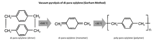
Figure 2 Polymerization route for poly-para-xylylene (Parylene N – C16H16)
De-Masking: Once the substrate conformal coating process is finalized substrates are de-masked by peeling off of the adhesive tape. This step is also critical and must be done with care not to damage the parylene around the masking tape.
Final Inspection (thickness, uniformity): Once the production processes are completed a final inspection is performed. These inspections are done via different routes such as visual inspection for issues ( uniformity, coating in keep out areas etc.), optical microscopy, and thickness control using a glass slide.
To learn more about parylene, download our whitepaper now:
Parylene for Electronics Whitepaper
Comments
Homepage 4/17/2020. 10:17:10 AM
... [Trackback] [...] Informations on that Topic: blog.paryleneconformalcoating.com/whats-the-difference-between-potting-and-conformal-coating/ [...]
londondrugscanada.bigcartel.comlondon-drugs 4/17/2020. 10:17:10 AM
cialis uk https://londondrugscanada.bigcartel.com/london-drugs This is nicely expressed. !